6
FN4640.5
November 18, 2004
Adjusting the Fault Reporting and Power
Supply Latch-Off Delay Times
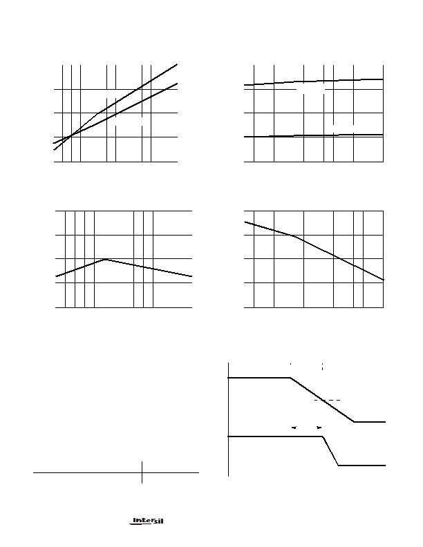
Figure 5 illustrates the relationship between the FLTN signal
and the gate drive outputs. Duration a, indicates the time
between FLTN starting to transition from High to Low,
(indicating a fault has occurred) and the start of the gate
drive outputs latching off. The latch-off is initiated by the
falling FLTN signal reaching the output latch threshold
voltage, VFLTN, TH. For additional details and wave forms
see HIP1011A Data Sheet FN4631. Table 1 illustrates the
effect of the FLTN capacitor on the response times.
Typical Performance Curves
FIGURE 1. r
ON
vs TEMPERATURE
FIGURE 2. OC VTH vs TEMPERATURE (VR
OCSET
= 1.21V)
FIGURE 3. OCSET CURRENT vs TEMPERATURE
FIGURE 4. V
CC
POWER ON RESET VTH vs TEMPERATURE
340
320
300
280
260
0 5 10 15 20 25 30 35 40 45 50 55 60 65 70
1000
900
800
700
600
TEMPERATURE (
o
C)
PMOS +12 r
ON
NMOS -12 r
ON
105
95
85
75
65
0 5 10 15 20 25 30 35 40 45 50 55 60 65 70
TEMPERATURE (
o
C)
5V OCVTH
3V OCVTH
102
101
100
99
98
0 5 10 15 20 25 30 35 40 45 50 55 60 65 70
TEMPERATURE (
o
C)
9.5
9.4
9.3
9.2
9.1
0 5 10 15 20 25 30 35 40 45 50 55 60 65 70
TEMPERATURE (
o
C)
TABLE 1. RESPONSE TIME TABLE
0.001?/SPAN>F
0.1?/SPAN>F
10?/SPAN>F
3V5VG Response a
0.85祍
37祍
3.8ms
FIGURE 5. TIMING DIAGRAM
3V5VG
FLTN
a
T1
T2
V
FLTN,TH
HIP1011B
发布紧急采购,3分钟左右您将得到回复。
相关PDF资料
HIP1020CK-T
IC CTRLR HOT PLUG SOT23-5
HIP6018BCBZ-T
IC REG TRPL BCK/LINEAR 24-SOIC
HIP6021CB-T
IC REG QD BCK/LINEAR 28-SOIC
HIP6521CB-T
IC REG QD BCK/LINEAR SYNC 16SOIC
HMC920LP5E
IC CTRLR ACTIVE BIAS 32QFN
IDTTSE2002B3CNRG
IC TEMP SENS EEPROM DFN-8
IPM6220ACAZ-T
IC REG 5OUT BUCK/LDO SYNC 24SSOP
IR2170
IC CURRENT SENSE 600V 1MA 8-DIP
相关代理商/技术参数
HIP1011BCBZA
功能描述:热插拔功率分布 W/ANNEAL PCI HOT PLUG PWR CNTRLR RoHS:否 制造商:Texas Instruments 产品:Controllers & Switches 电流限制: 电源电压-最大:7 V 电源电压-最小:- 0.3 V 工作温度范围: 功率耗散: 安装风格:SMD/SMT 封装 / 箱体:MSOP-8 封装:Tube
HIP1011BCBZA-T
功能描述:热插拔功率分布 W/ANNEAL PCI HOT PLUG PWR CNTRLR RoHS:否 制造商:Texas Instruments 产品:Controllers & Switches 电流限制: 电源电压-最大:7 V 电源电压-最小:- 0.3 V 工作温度范围: 功率耗散: 安装风格:SMD/SMT 封装 / 箱体:MSOP-8 封装:Tube
HIP1011CB
功能描述:IC CTRLR HOT PLUG PCI 16-SOIC RoHS:否 类别:集成电路 (IC) >> PMIC - 热交换 系列:- 产品培训模块:Obsolescence Mitigation Program 标准包装:100 系列:- 类型:热插拔开关 应用:通用 内部开关:是 电流限制:可调 电源电压:9 V ~ 13.2 V 工作温度:-40°C ~ 150°C 安装类型:表面贴装 封装/外壳:10-WFDFN 裸露焊盘 供应商设备封装:10-TDFN-EP(3x3) 包装:管件
HIP1011CB-T
功能描述:IC CTRLR HOT PLUG PCI 16-SOIC RoHS:否 类别:集成电路 (IC) >> PMIC - 热交换 系列:- 产品培训模块:Obsolescence Mitigation Program 标准包装:100 系列:- 类型:热插拔开关 应用:通用 内部开关:是 电流限制:可调 电源电压:9 V ~ 13.2 V 工作温度:-40°C ~ 150°C 安装类型:表面贴装 封装/外壳:10-WFDFN 裸露焊盘 供应商设备封装:10-TDFN-EP(3x3) 包装:管件
HIP1011CB-TS2568
制造商:Rochester Electronics LLC 功能描述: 制造商:Intersil Corporation 功能描述:
HIP1011CBZA
功能描述:热插拔功率分布 W/ANNEAL PWR DIST CNTRLR 16LD N RoHS:否 制造商:Texas Instruments 产品:Controllers & Switches 电流限制: 电源电压-最大:7 V 电源电压-最小:- 0.3 V 工作温度范围: 功率耗散: 安装风格:SMD/SMT 封装 / 箱体:MSOP-8 封装:Tube
HIP1011CBZA-T
功能描述:热插拔功率分布 W/ANNEAL PWR DIST CNTRLR 16LD N RoHS:否 制造商:Texas Instruments 产品:Controllers & Switches 电流限制: 电源电压-最大:7 V 电源电压-最小:- 0.3 V 工作温度范围: 功率耗散: 安装风格:SMD/SMT 封装 / 箱体:MSOP-8 封装:Tube
HIP1011D
制造商:INTERSIL 制造商全称:Intersil Corporation 功能描述:Dual PCI Hot Plug Controller